Diamond CVD
Cardiff Diamond Foundry operates four Microwave Plasma Chemical Vapour Deposition systems. Our main doping workhorse is a Seki 6500 series system equipped with Trimethylboron as the doping source. This reactor routinely grows superconducting diamond films with transition temperatures around 5K as well as electrochemical electrode grade material. A second load-locked UHV system (Seki SDS5250) is mainly used for our SQUIDs and superconducting nanoelectromechanical systems. For intrinsic diamond growth we operate a Carat Systems CTS6U which is basically an enhanced 6500 series with differentially pumped seals and conflat windows. It has a far lower leak rate than a standard 6500 reactor. Our fourth reactor is a home built quartz tube (NIRIM) style reactor. This system is for the production of diamond with novel colour centres. We openly share the design of this system to other users. This system has a liquid precursor option for incorporating novel materials into the CVD process. Our open source design is available at this wiki.
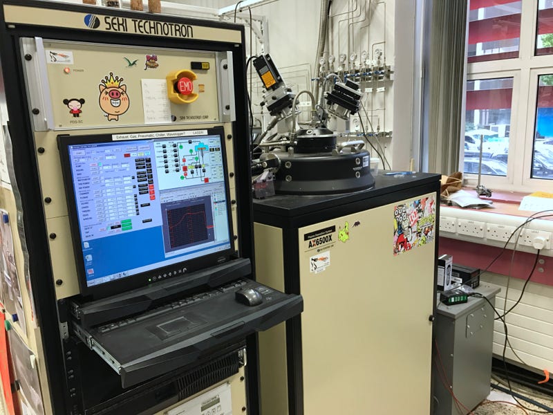

Our two boron doping systems, above left general purpose Seki 6500 system for routine production and above right, our load locked Seki SDS5250 for SQUID development.
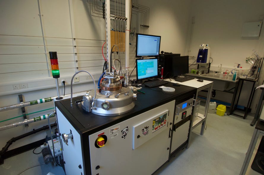
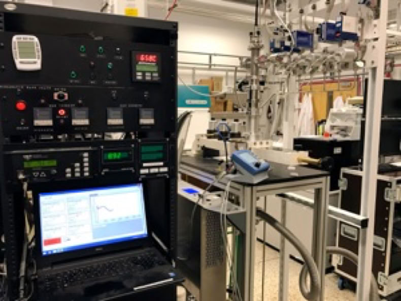
Above left: Our intrinsic reactor, Carat systems CTS6U. Above right: our home built quartz tube reactor, for more information including full design schematics see wiki here and Thomas et al, AIP Advances, 8 (2018) 035325
All reactors have comprehensive in-situ monitoring including pyrometers covering the temperature ranges 200-600ºC, 300-1000ºC, 475-1475ºC and 800-1800ºC. These are two colour / ratio pyrometers which have been calibrated and demonstrated their accuracy on numerous substrates. We have multiple wavelengths for different materials (1-5µm) as well as IR cameras and a disappearing filament pyrometer. This is not without error, diamond is not a black body emitter as it is highly transparent across the available IR / visible pyrometer spectrum.
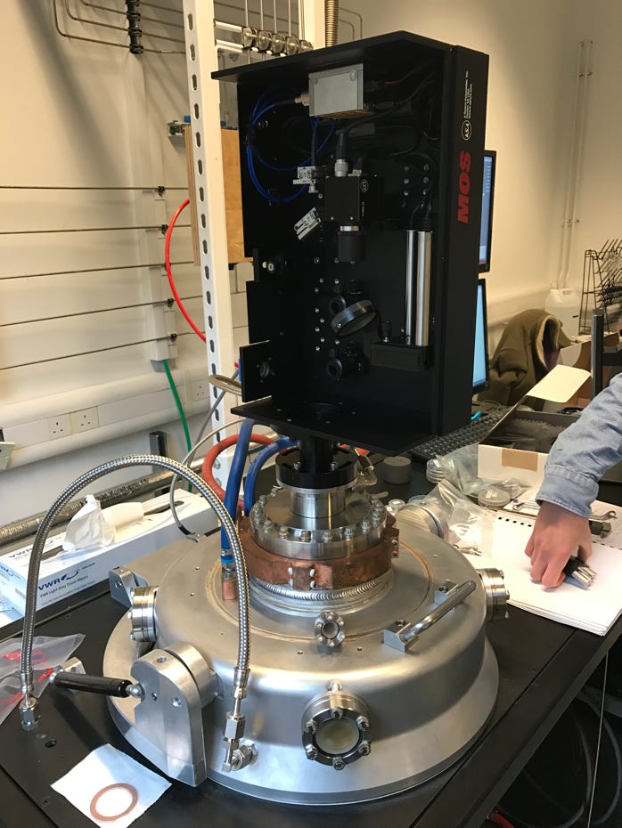
Growth rates can be monitored in-situ either by laser interferometry (for films thicker than 100nm) or by Spectroscopic Ellipsometry (films from 10nm thick). We also operate a k-Space MOS for in-situ stress characterisation (see left, where it is situated on our CTS6U).
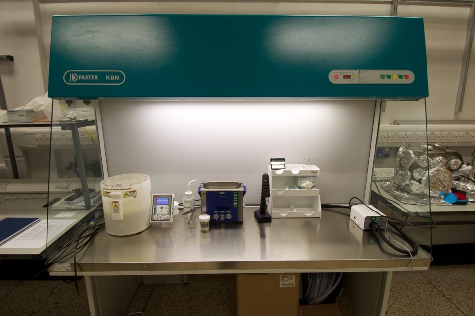
Nucleation areas are entirely under (class 100) lamina flow to reduce contamination from dust particles etc (above right). Substrates are immersed in aqueous colloids of mono-disperse diamond particles under ultrasound. After this they are rinsed and spun dry with a wafer spinner. These techniques have been demonstrated to yield the ultra-high nucleation densities required for nanocrystalline diamond growth. See nanodiamond.
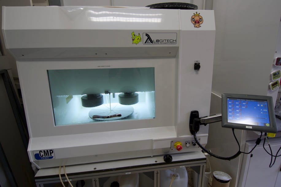
For post growth planarisation, the laboratory is equipped with a Logitech Tribo Chemo-Mechanical Polishing facility (left). Processes to planarise nanocrystalline diamond films from their as grown roughness of the order of 20 nm rms (over several micron) down to below 2nm rms (over 25 µm2) have been developed in collaboration with Logitech Ltd. This process is based around Syton SF1 slurry (colloidal silica). This process has been demonstrated to be effective on both nanocrystalline diamond and single crystal materials ({100} and {111}). See CMP.