Doping and Superconductivity
Perfect diamond is a very poor conductor of electricity, having an equivalent free electron density of one free electron in the volume of the earth. Of course, perfect diamonds do not exist, but diamond is still one of the best electrical insulators available. However, we can control the electrical conductivity of diamond by adding impurity atoms. This is called doping. As diamond is the most atomically dense materials (atoms are closer together in diamond than any other material), this is hard to do and generally quite inefficient. We can add boron atoms as they are smaller than carbon and this also makes the diamond blue. Boron does occur in natural diamond but it is relatively rare, a good example being the Hope Diamond.
Diamond that conducts electricity has a number of important applications. The most widespread would be electrochemical electrodes where it exhibits extreme stability, low noise and the widest potential window available. Such diamond electrodes are used for waste water treatment and cleaning swimming pool waters. These are being commercialised by Element6, Adamant Technologies etc. These electrodes are also very important for bio-sensing, allowing the detection of very small quantities of molecules such as pathogens (anthrax etc), neurotransmitters or DNA in solution. Doping with boron is also used to make semiconducting diamond which is being developed by other groups for electronic devices.
When diamond films which contain very large concentrations of boron (>0.25%) are cooled down to over 200 ºC below room temperature, they become superconducting, that is they offer no resistance to the flow of electricity. This is a very interesting phenomena, as pure diamond is extremely resistive to the flow of electricity, a common rule of thumb being there is less that one free electron per volume of the earth in a perfect diamond (theoretically).
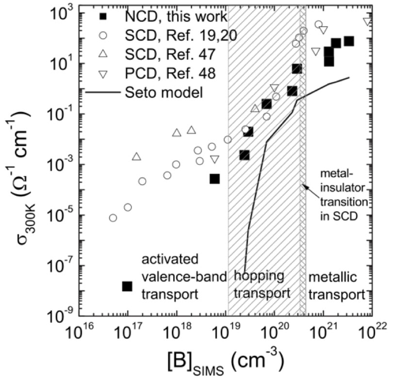
Cardiff Diamond Foundry has optimised the doping of diamond, mostly in Nanocrystalline Diamond (NCD), however we also grow doped single crystal and microcrystalline diamond. Below are some examples of conductivity versus temperature and boron concentration.


Left: Conductivity of diamond films vs boron concentration for NCD, SCD (single crystal diamond ) and PCD (microcrystalline / polycrystalline diamond). All three types of diamond exhibit similar behaviour except at low boron concentration where the conductivity of NCD drops off due to the small grain size, see Gajewski et al, PRB 79 (2009) 045206
Bottom left: Low temperature conductivity as a function of boron concentration, above a critical concentration (the Metal - Insulator Transition), these films exhibit superconductivity, see Achatz et al, PRB 79 (2009) 201203
Bottom right: recent optimised NCD films showing higher transition temperatures and superconductivity even in very thin films (the 35nm film is superconductivity at much lower temperatures), see Klemencic et al, PRM 1 (2017) 044801

Superconducting Devices
Our main motivation in developing superconducting nanocrystalline diamond films is for the fabrication of superconducting devices. NCD can easily be etched and nanostructured, and this allows the fabrication of such devices as Josephson Junctions and SQUIDs (see below). NCD exhibits a high Young’s modulus and can also be structured into high frequency mechanical resonators (see below).


Top Left: Plan view at low magnification of overall device structure and contact pads. The yellow shows the diamond after being patterned by ebeam lithography and reactive ion etching.
Middle left: Higher magnification of the above showing multiple SQUIDs with different size junctions. Each SQUID has multiple contacts for redundancy.
Bottom left: High magnification again showing an individual SQUID. The weak links (150-200 nm width junctions) are to the right of the device. The surface roughness of the diamond is clearly visible.
Bottom middle: Clear junction like behaviour of weak links (100 nm) within the SQUID. The junctions show clear hysteresis.
Bottom right: Low field oscillations of the critical current with period 0.3 mT. These devices also operate under fields up to 4 T, this is the highest magnetic field operation (at normal incidence) of a SQUID reported.


Top Left: Superconducting nano cantilever fabricated from boron doped NCD. The device was fabricated by growing boron doped NCD on silicon with a 500nm SiO2 interlayer. After ebeam pattering a reactive ion etching, the device is released by sacrificially etching the SiO2 with HF vapour.
Bottom left: The resonant frequency of the superconducting cantilever as a function of magnetic field. The ability of the device to operate at high magnetic field is surprising and due to the inherent high critical field of boron doped diamond.
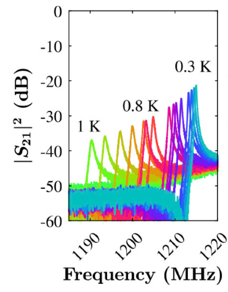
We have also demonstrated coplanar resonators fabricated from similar superconducting NCD to the above SQUIDs, Josephson Junctions and cantilevers. These devices exploit that fact that although superconductors exhibit no electrical resistance, they have non-zero impedance. This impedance includes a small contribution from quasiparticles (electrons not bound as Cooper pairs) and thus the breaking of Cooper pairs by radiation /temperature etc can be detected by changes in the natural frequency of a resonant circuit. Below is an optical image of a coplanar resonator etched from thin film boron doped NCD, through to its float zone silicon substrate.


Above left to right: Scanning Electron Micrographs of increasing magnification of the coplanar resonator. The smooth areas represent where the NCD has been etched though to the substrate.
Left: Resonance characteristics of the above coplanar waveguide. The resonant peaks shift as a function of temperature as the concentration of quasi-particles and thus the impedance varies with temperature.