Diamond growth
Diamond growth has evolved from an academic curiosity to an industrial process, with several companies selling various forms of high quality diamond. Diamond can be grow by several techniques ranging from the mimicking of nature in High Pressure / High Temperature (HPHT) growth to the metastable processes of Chemical Vapour Deposition (CVD) which cheats nature.
In HPHT growth, pressures greater than 100000 bar and temperatures greater than 2000 ºC are used to grow diamond under conditions similar to those found in the earths crust. These conditions are basically the extreme conditions under which diamond is favourable over graphite in the carbon phase diagram. Diamond growth in nature occurs over millions of years and so a catalyst must be used in order to make the process viable. HPHT processes can unfortunately only produce small crystals of the order of several carats / tens of cubic millimetres and thus are limited in application. That said it is still by far the most produced form of diamond which dominates the cutting tool and wire drawing die market.
CVD growth is executed under conditions which are actually more thermodynamically favourable to graphite growth than diamond. Diamond growth is possible due to the very special behaviour of atomic hydrogen. Atomic hydrogen terminates the surface of diamond, maintaining its structure and restricting its conversion into graphite. It also etches graphitic carbon over fifty times more efficiently that diamond. Thus the growth is actually metastable with both allotropes of carbon growing simultaneously but with the enhanced etching of non - diamond carbon. Being a low pressure gas phase process, CVD has a number of advantages over HPHT. Very high purity diamonds, exceeding anything nature can offer can be grown. Foreign elements can be introduced into the growth, such as boron to make blue diamond, or nickel/nitrogen to generate single photon emitters for quantum computing applications.
CVD is possible over large areas, but the growth of single crystal diamond is only possible on other single crystals and thus is limited by the available substrate. Growth of diamond on non diamond substrates results in polycrystalline material, a film comprising of many smaller crystals. The size of these crystals determines many of their properties, from very close to the best single crystal diamond to graphitic like properties. Thus material properties can be manipulated by the growth process in many ways.
CVD is an area of active research at Cardiff Diamond Foundry (see details of our growth facility here). We focus on developing solutions that are not commercially available, such as the integration of diamond with novel materials (such as GaN) and in-situ monitoring. We also specialise in doping with boron, superconductivity as well as post growth planarisation (see CMP). We have a long track record developing Nanocrystalline Diamond (NCD, see below), a thin film version of diamond with many of the extreme properties of diamond but at drastically reduced cost. Below are some examples of the materials we grow and process.
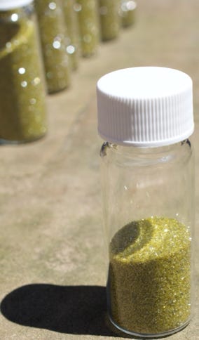
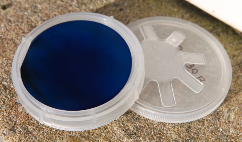
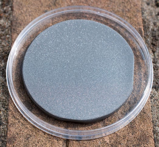
Left to Right: HPHT grit, the colour is yellow due to the high concentration of nitrogen; thin Nanocrystallline Diamond (NCD) on silicon, the blue colour is due to light interferometry effects between the diamond and the silicon; Microcrystalline Diamond (µCD), the sparkle originates from light scattering off the large crystals.
Nanocrystalline Diamond films
Nanocrystalline diamond (NCD) is a thin film of diamond with nanometre size crystals, usually supported on a silicon wafer. However, NCD can be grown on many other substrates such as metals, quartz and other transparent glasses, piezoelectrics etc. NCD has most of the extreme properties of diamond but at a substantially reduced cost, larger area and more practical format. These films are grown by Microwave Plasma Chemical Vapour Deposition (CVD) under low pressures (see Diamond Growth).
NCD has many diverse applications. The extreme mechanical properties of diamond make it an ideal material for Nano/Micro-Electro-Mechanical Systems. Its low friction and wear properties make it an advanced tribological coating. The surface stability, chemical inertness and electrochemical properties are currently being exploited for bio-sensing. A review of the growth and applications of NCD is available here.
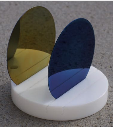
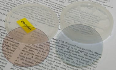
The images right show examples of NCD films on silicon and quartz (2” diameter), the different colours are due to their different thicknesses.
